��������
�о��������òġ�MEMSר�� GM1050
�������ڣ�2024/11/26 16:48:12
��������� �������� �ղ����� ��ע���� ����һ���� ���ٱ��� ���ղء� ����ע���о��������òġ�MEMSר�� GM1050
Gersteltec SU-8 series
������о̩�ƹ������˾
��Ʒ���������� :13��23��66554 �ۿۣ�35��9123��
������о̩�ƹ������˾��������2014�꣬��һ�ҷ�������������IJ�Ʒó�����������ṩ�̡������Ѿ���Ϊ���������Ƴ��������ش�ѧ�о��������ĺ�����飻��˾�������ҳ�̬�ȶԴ��¾ɿͻ����Կͻ�����Ϊ�����ṩ���ʸ�Ч�ʵ�רҵ�����ṩ��Ʒ����������֧Ԯ�������������Ŀ���dz�Ϊһ���²���Ӧ�ü����ƹ�����רҵ��Ӧ�̡�
��Ҫ��Ʒ��Χ ��
һ�� ��̣����Թ�̽����Թ�̽�
���� ��������������Ϳ�㡢��Բ�и�����ͼ��Ͻ�
���� ����������ѧƷ����ӰҺ����ϴ����ȥ��Һ�Ͱ���Һ
Gersteltec SU-8 series
GM1050��negative tone photo-epoxy
for layers 3 to 8 ��m��
General information
GM 1050 is an epoxy based, chemically amplified resist system with excellent
sensitivity high aspect ratios. The primary applications are Micro-fabricated
Mechanical Structures (MEMS) other Microsystems.
Examples are sensors, micro-fluidic components, electronic coils, inkjet print head
nozzles, multi-chip modules, actuators, LCD spacers moulds for plastic, stamps
for hot embossing electroplating.
Datasheet parts��
1 /Schematics of the process
2 /Process description
3 /Process parameters
4 /Processing GM 1050�C Overview
5 /Typical processes (3, 4, 5, 6, 7 & 8 ��m)
6 /Troubleshooting
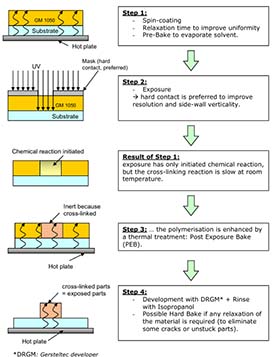
1/Schematicsoftheprocess
2 /Process description
A typical GM 1050 process consists of
-
Substrate preparation (dehydration, cleaning��)
- Spin-coating
- Relaxation time to improve the surface uniformity
- Soft Bake
Exposure to initiate the cross-linking
- Post Exposure bake (PEB), to cross-link exposed regions.
- Development
Rinse & dry
- Hard Bake (optional: in case of contact with liquids)
- Imaged material (optional: in case of moulding)
- Remove (optional: in case of moulding)
(in chronological order)
? Put the substrate in an oven at a minimum temperature of 130��C during at
least 20 minutes to remove adsorbed water the substrate surface.
Alternatively use an oxygen plasma for 7 min at 500 Watts in a Microwave
plasma reactor. This should increase the temperature inside the plasma
chamber above 80��C after the 2 first minutes.
Stard HMDS procedure is not recommended for GM10xx series on SiO2
based wafers.
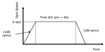
? Spin-coat the resist after cooling down the substrates, at the wanted speed
level during 40 seconds. The acceleration deceleration ramps should be
about 100 rpm/s to avoid any contamination of the chuck the pins by the
GM 1050. Otherwise, some resist on the vacuum system should damage your
spin coat system.
? Relax (optional) the resist 5 min. depending on the resist thickness. For
GM 1050, this step is not necessary. If there are some bubbles just after spin
coating they can be burst using a clean thin tip. The created hole should be
removed during the required time. Finally this relaxation time should improve
the uniformity of the layer, evaporate some portion of solvent.
? Softbake the coated substrate directly on a hotplate at 120��C during the
requested time. If some bubbles appear, make a ramp of about 4��C/min., or
make a step at 65��C during 30s. When holding them with some tweezers no
stick or impression have to be observed otherwise increase the bake time.
Cooling on a room temperature plate.
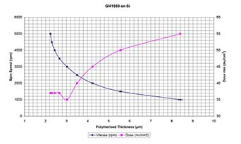
? Expose the coated substrate with the mask. The exposure dose adjusts the
negative wall profile whose slope is closed to 90��. Have a look on the exposure
curve to choose as a function of your thickness the minimum dose (at i-line).
Ideally
try some multiple exposures above the minimum dose.
? Post Exposure Bake (PEB): that bake accelerates the cross-linking of the
exposed areas making them insoluble in the developer. Bake at 95��C during the
requested time with a ramp of 4��C/min. Use the same ramp for cooling down to
room temperature.
? Develop in DRGM. When the structure is through-developed (cleared), add
another 10% of the time in a cleaned bath of the total development time to
finalize the side wall profile. An over-development induces adhesion problems.
? Rinse with Isopropanol. Once there are not any more white traces the
development is then finished; otherwise develop again.
? Dry the wafers just letting them at the ambient air, on a wet bench with an
appropriate air flow (exhaust) or use a nitrogen flow.
? Hard-bake (optional) the coated substrate if after drying there are some
unstuck GM 1050 or cracks. Only the smallest cracks (<5 ��m) will be totally
removed after this step. Recommended bake: 2��C/min room temperature
up to 150��C, isotherm during 5 to 10 min., natural cooling (4��C/min max).
Optional��
? Imaged material (optional: in case of moulding): deposition of you material by
sputtering, electrodepositing��
? RemoveGM1050: using the Gersteltec GM 1050 striper (without hard-bake).
3 /Process parameters
4/ProcessingGM1050-Overview
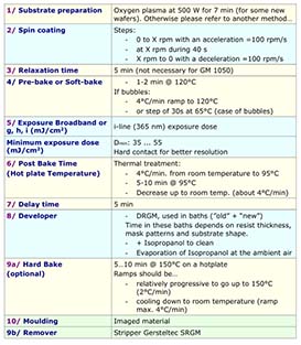
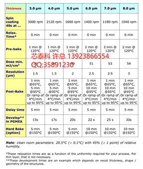
5/Typicalprocesses(3,4,5,6,78��m)
Firstly,thewaferpreparationshouldbeasmentionedpreviously(Oxygenplasmaat
500Wfor7min(forsomecleanedwafersyet)��).
6 /Troubleshooting
? Cracks: these drawbacks appear as a function of the exposure dose,
temperature ramps taken Pre-bake time. to make above the minimum dose
(cf.��5) to define the right dose 20% more should be enough.
? White traces after development: This is only because there is still some
unexposed GM 1050 not totally developed. In fact unexposed GM
1050+Isopropanol make a white complex that you can find on your wafers.
In the other side, just pay attention to not develop too much time. Otherwise
you could unstick the GM 1050 layer the substrate.
Appendix
Equipments:
-Spin-coating
: RC-8 Karl Suss
-Mask aligner
: MA6 mask aligner Karl Suss
- Hotplates
Karl Suss
- Thickness measurements
: AlphaStep 500.